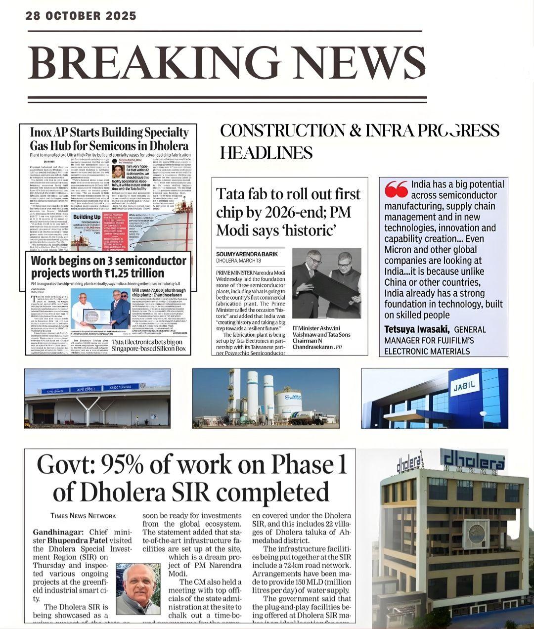
2D Carbon Carbon Plate: Advanced Material Solutions by Zhejiang Dehong Carbon Fiber Composite Material Co., Ltd.
Zhejiang Dehong Carbon Fiber Composite Material Co., Ltd. is at the forefront of delivering innovative and high-performance materials for industries that demand the best in thermal and mechanical properties. One of the standout products from the company is the 2D Carbon Carbon Plate, a revolutionary material that combines high strength, exceptional heat resistance, and durability, making it ideal for a variety of high-stress applications in aerospace, automotive, energy production, and manufacturing.
2D Carbon Carbon Plate
https://en.zhejiangdehong.com/carbon-carbon-cover-plate.html
What is the 2D Carbon Carbon Plate?
The 2D Carbon Carbon Plate is a composite material made from carbon fibers embedded in a resin matrix. After undergoing a specialized heat treatment process, the plate becomes a robust, lightweight, and heat-resistant material capable of performing in extremely high temperatures and mechanical stress conditions. This transformation enhances the material's structural integrity, making it perfect for use in industries that require durable, high-performance materials.
Key Features of the 2D Carbon Carbon Plate
Exceptional Heat Resistance
One of the most important features of the 2D Carbon Carbon Plate is its superior heat resistance. Capable of enduring temperatures up to 3,000°C, this material excels in applications that involve exposure to extreme heat. It is often used in aerospace for components like heat shields, turbine blades, and rocket nozzles, where the ability to maintain structural integrity at high temperatures is critical. In addition, the 2D Carbon Carbon Plate is ideal for use in energy production systems, such as nuclear reactors and high-temperature furnaces, where maintaining thermal stability is essential.
Strength-to-Weight Ratio
The 2D Carbon Carbon Plate is known for its excellent strength-to-weight ratio. It is significantly lighter than traditional metals while maintaining high mechanical strength, making it an ideal choice for industries where reducing weight without sacrificing strength is crucial. For instance, in the aerospace and automotive industries, lightweight materials help reduce fuel consumption and increase speed and performance. The 2D Carbon Carbon Plate is a go-to material for applications where weight reduction plays a pivotal role in enhancing overall system efficiency.
Durability and Longevity
Durability is another key advantage of the 2D Carbon Carbon Plate. This material is highly resistant to wear, corrosion, and thermal cycling, ensuring it can withstand long-term exposure to harsh environments. Whether it is subjected to extreme temperatures or repeated mechanical stresses, the 2D Carbon Carbon Plate maintains its strength and integrity over time. This makes it a cost-effective material for industries that require materials to perform reliably without frequent replacements or maintenance.
Versatility Across Multiple Industries
The 2D Carbon Carbon Plate is a versatile material with applications across various industries:
Aerospace: In aerospace, the 2D Carbon Carbon Plate is used for components exposed to high heat and stress, such as rocket nozzles, heat shields, and turbine blades. It ensures structural stability and reliability in critical aerospace systems.
Automotive: The 2D Carbon Carbon Plate is increasingly used in high-performance automotive applications, including electric cars and racing vehicles, where reducing weight and maintaining strength are key to performance. This helps improve fuel efficiency, handling, and speed.
Energy Production: In energy production, the 2D Carbon Carbon Plate is vital for components in high-temperature power generation systems, such as reactors, furnaces, and solar thermal plants. Its heat resistance and durability make it an excellent choice for ensuring operational efficiency and safety.
Industrial Manufacturing: The 2D Carbon Carbon Plate is used in industrial applications like metal forging, semiconductor production, and ceramics, where thermal stability and mechanical strength are required for optimal performance.
Customizable to Fit Specific Needs
Zhejiang Dehong offers customizable 2D Carbon Carbon Plates to meet the specific needs of various applications. Whether you need plates with customized sizes, thicknesses, or specific properties tailored to your industry’s requirements, Zhejiang Dehong can provide a solution that aligns perfectly with your operational needs.
2D Carbon Carbon Plate: Advanced Material Solutions by Zhejiang Dehong Carbon Fiber Composite Material Co., Ltd.
Zhejiang Dehong Carbon Fiber Composite Material Co., Ltd. is at the forefront of delivering innovative and high-performance materials for industries that demand the best in thermal and mechanical properties. One of the standout products from the company is the 2D Carbon Carbon Plate, a revolutionary material that combines high strength, exceptional heat resistance, and durability, making it ideal for a variety of high-stress applications in aerospace, automotive, energy production, and manufacturing.
2D Carbon Carbon Plate
https://en.zhejiangdehong.com/carbon-carbon-cover-plate.html
What is the 2D Carbon Carbon Plate?
The 2D Carbon Carbon Plate is a composite material made from carbon fibers embedded in a resin matrix. After undergoing a specialized heat treatment process, the plate becomes a robust, lightweight, and heat-resistant material capable of performing in extremely high temperatures and mechanical stress conditions. This transformation enhances the material's structural integrity, making it perfect for use in industries that require durable, high-performance materials.
Key Features of the 2D Carbon Carbon Plate
Exceptional Heat Resistance
One of the most important features of the 2D Carbon Carbon Plate is its superior heat resistance. Capable of enduring temperatures up to 3,000°C, this material excels in applications that involve exposure to extreme heat. It is often used in aerospace for components like heat shields, turbine blades, and rocket nozzles, where the ability to maintain structural integrity at high temperatures is critical. In addition, the 2D Carbon Carbon Plate is ideal for use in energy production systems, such as nuclear reactors and high-temperature furnaces, where maintaining thermal stability is essential.
Strength-to-Weight Ratio
The 2D Carbon Carbon Plate is known for its excellent strength-to-weight ratio. It is significantly lighter than traditional metals while maintaining high mechanical strength, making it an ideal choice for industries where reducing weight without sacrificing strength is crucial. For instance, in the aerospace and automotive industries, lightweight materials help reduce fuel consumption and increase speed and performance. The 2D Carbon Carbon Plate is a go-to material for applications where weight reduction plays a pivotal role in enhancing overall system efficiency.
Durability and Longevity
Durability is another key advantage of the 2D Carbon Carbon Plate. This material is highly resistant to wear, corrosion, and thermal cycling, ensuring it can withstand long-term exposure to harsh environments. Whether it is subjected to extreme temperatures or repeated mechanical stresses, the 2D Carbon Carbon Plate maintains its strength and integrity over time. This makes it a cost-effective material for industries that require materials to perform reliably without frequent replacements or maintenance.
Versatility Across Multiple Industries
The 2D Carbon Carbon Plate is a versatile material with applications across various industries:
Aerospace: In aerospace, the 2D Carbon Carbon Plate is used for components exposed to high heat and stress, such as rocket nozzles, heat shields, and turbine blades. It ensures structural stability and reliability in critical aerospace systems.
Automotive: The 2D Carbon Carbon Plate is increasingly used in high-performance automotive applications, including electric cars and racing vehicles, where reducing weight and maintaining strength are key to performance. This helps improve fuel efficiency, handling, and speed.
Energy Production: In energy production, the 2D Carbon Carbon Plate is vital for components in high-temperature power generation systems, such as reactors, furnaces, and solar thermal plants. Its heat resistance and durability make it an excellent choice for ensuring operational efficiency and safety.
Industrial Manufacturing: The 2D Carbon Carbon Plate is used in industrial applications like metal forging, semiconductor production, and ceramics, where thermal stability and mechanical strength are required for optimal performance.
Customizable to Fit Specific Needs
Zhejiang Dehong offers customizable 2D Carbon Carbon Plates to meet the specific needs of various applications. Whether you need plates with customized sizes, thicknesses, or specific properties tailored to your industry’s requirements, Zhejiang Dehong can provide a solution that aligns perfectly with your operational needs.
0 Commentarios
0 Acciones
146 Views
0 Vista previa